Advanced Etching and Fabrication Equipment: A comprehensive guide to industry-leading technologies
Introduction
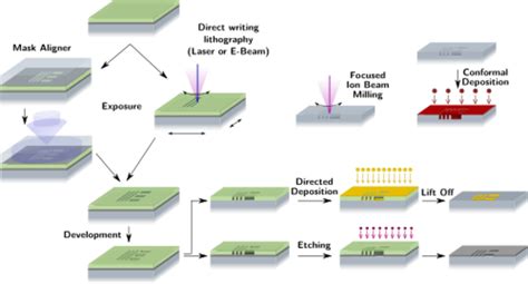
Etching and Fabrication are fundamental processes in the semiconductor, electronics, and MEMS industries. They involve precisely shaping and structuring materials on the nanoscale, enabling the creation of complex devices such as integrated circuits (ICs), transistors, sensors, and other electronic components. This article provides a comprehensive overview of the latest etching and fabrication equipment, highlighting the key technologies, benefits, and applications.
Etching and Fabrication Technologies
Dry Etching
This process uses plasma or ion beams to remove material in a controlled manner. It offers high-precision, anisotropic etching, making it suitable for creating vertical or slanted sidewalls in semiconductors. Common dry etching techniques include:
-
Reactive Ion Etching (RIE): Uses plasma containing reactive gases to etch materials.
-
Deep Reactive Ion Etching (DRIE): A specialized RIE technique that achieves high aspect ratios and depths.
-
Cryogenic Etching: Uses chilled plasma gases to minimize heat-induced damage and improve etch selectivity.
Wet Etching
This process involves immersing the substrate in a liquid chemical solution that selectively dissolves the desired material. Wet etching offers low cost and simplicity but is less precise than dry etching.
-
Isotropic Etching: Produces uniform etching in all directions.
-
Anisotropic Etching: Etches preferentially in specific crystallographic orientations, creating sidewalls of different angles.
Etching and Fabrication Equipment
Etchers
Etchers are the core equipment used in etching processes. They typically consist of plasma or RF generators, etching gases, and a vacuum chamber to maintain the etching environment. Advanced etchers offer features such as:
-
Advanced process control: Automated control systems to optimize etch parameters and minimize defects.
-
Multi-step etching: Capability to perform multiple etching steps in a single process, increasing throughput.
-
In-situ metrology: Sensors for real-time monitoring of etch rates and uniformity.
Deposition Equipment
Used for adding or modifying materials on the substrate, deposition equipment involves techniques such as:


-
Chemical Vapor Deposition (CVD): Deposits thin films from gaseous precursors.
-
Physical Vapor Deposition (PVD): Deposits thin films by physical processes such as evaporation or sputtering.
-
Atomic Layer Deposition (ALD): An advanced technique that deposits ultrathin films with precise control.
Inspection Equipment
Critical for quality control, inspection equipment uses optical or electron microscopy to analyze etched and fabricated structures. Advanced tools offer:
-
High resolution: Ability to resolve features on the nanometer scale.
-
3D reconstruction: Creating detailed 3D models of samples.
-
Automated defect detection: Software algorithms for identifying and classifying defects.
Benefits and Applications
Benefits of Advanced Etching and Fabrication Equipment
-
Improved precision and accuracy: Enables the creation of intricate structures with high dimensional control.
-
Increased throughput: Advanced tools offer faster etching and deposition rates, reducing production time.
-
Enhanced quality: Minimizes defects and improves the performance of fabricated devices.
-
Versatility: Supports a wide range of materials and processes, allowing for complex device designs.
Applications
Etching and fabrication equipment are essential in the following industries:
-
Semiconductors: Fabrication of ICs, transistors, and memory devices.
-
Electronics: Production of printed circuit boards, displays, and sensors.
-
MEMS: Creation of microelectromechanical systems for medical, automotive, and aerospace applications.
-
Biotechnology: Fabrication of biosensors, lab-on-a-chip devices, and drug delivery systems.
Common Mistakes to Avoid
-
Overetching: Etching for too long, leading to undercutting or weakening of structures.
-
Anisotropic etch control: Failing to control the directionality of etching, resulting in non-vertical sidewalls.
-
Process contamination: Introducing impurities into the etching or deposition environment, affecting device performance.
-
Insufficient cleaning: Incomplete cleaning after etching or deposition, leading to residual contamination.
-
Improper handling: Incorrect handling of wafers or samples can cause damage or defects.
Step-by-Step Approach to Etching and Fabrication
1. Substrate Preparation
- Clean the substrate to remove any contaminants.
- Apply a photoresist or mask to define the areas to be etched.
2. Etching
- Load the substrate into the etcher.
- Set and optimize the etching parameters (pressure, gas flow, power).
- Monitor the etching process using in-situ metrology.
3. Deposition (optional)
- Deposit thin films or materials as needed using a suitable deposition technique.
4. Inspection
- Inspect the etched and/or deposited structure using microscopy or other analysis methods.
- Verify dimensional accuracy, surface quality, and defect density.
5. Post-processing
- Remove the photoresist or mask.
- Perform additional steps such as cleaning, annealing, or passivation.
Comparison of Pros and Cons
Dry Etching vs. Wet Etching
| Feature |
Dry Etching |
Wet Etching |
| Precision |
Higher |
Lower |
| Anisotropy |
Higher |
Lower |
| Etching rate |
Slower |
Faster |
| Cost |
Higher |
Lower |
| Environmental impact |
Less hazardous |
More hazardous |
R&D Trends and Future Outlook
The etching and fabrication industry is constantly evolving, with ongoing research and development focused on:
-
Advanced materials: Developing new materials with improved etch resistance and deposition properties.
-
Innovative etching techniques: Exploring novel methods such as maskless etching and laser-assisted etching.
-
Integration and automation: Enhancing the integration of equipment and automating processes to improve efficiency.
-
Nanometer-scale precision: Pushing the limits of dimensional control for the creation of ultra-small devices.
Market Size and Statistics
According to Market Research Future, the global etching and fabrication equipment market is projected to reach $59.2 billion by 2030, growing at a CAGR of 7.4% from 2023-2030. The Asia-Pacific region is the largest market, driven by the growth of the electronics and semiconductor industries.
Tables
Table 1: Market Share of Leading Etching Equipment Manufacturers
| Manufacturer |
Market Share |
| Lam Research |
32% |
| Applied Materials |
28% |
| Tokyo Electron |
20% |
| ASM International |
10% |
| Samsung Electronics |
5% |
Table 2: Etching Techniques and Applications
| Technique |
Application |
| RIE |
Silicon etching, metal patterning |
| DRIE |
Deep trench etching, MEMS fabrication |
| Cryogenic Etching |
High-aspect ratio etching, damage reduction |
| Isotropic Wet Etching |
Polishing, wafer cleaning |
| Anisotropic Wet Etching |
Crystallographic orientation-dependent etching |
Table 3: Key Specifications of Advanced Deposition Equipment
| Parameter |
Specification |
| Process |
CVD, PVD, ALD |
| Film uniformity |
|
| Thickness control |
|
| Deposition rate |
> 50 nm/min |
| Chamber temperature |
|
Conclusion
Etching and fabrication equipment are essential tools for manufacturing advanced semiconductor devices, electronic components, and MEMS systems. By understanding the key technologies, benefits, and applications, researchers, engineers, and manufacturers can harness these tools to create innovative products and drive technological advancements. With ongoing R&D and industry growth, the future of etching and fabrication looks bright, promising continued advancements and transformative technologies.
